Printed Circuit Boards (PCBs) are the backbone of modern electronics. From smartphones and computers to cars and medical devices, almost every gadget we use today relies on PCBs to function. But how exactly are these boards made? If you’re new to the topic, this guide will walk you through what PCB manufacturing is, why it’s important, and the step-by-step process that brings these essential components to life.
Understanding PCB Manufacturing
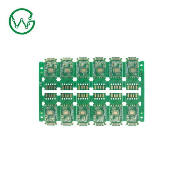
PCB manufacturing is the process of designing and producing printed circuit boards that connect electronic components. These boards are made from insulating materials, usually fiberglass, with conductive pathways etched or printed onto them. The purpose of a PCB is to provide mechanical support and an organized layout for electronic components while allowing electrical signals to pass between them efficiently.
Unlike old wiring methods, PCBs simplify circuits by integrating copper traces onto a single board, making devices smaller, faster, and more reliable.
Why PCBs Are Important in Electronics
PCBs play a vital role in modern electronics for several reasons:
- Miniaturization: They allow complex circuits to be fitted into compact devices like smartphones and laptops.
- Durability: The design ensures stable and long-lasting performance under different conditions.
- Mass Production: Once a design is created, it can be replicated at scale with high precision.
- Efficiency: PCBs reduce wiring errors and ensure smoother connections between components.
Without PCB technology, electronic devices would be bulkier, less reliable, and far more expensive to produce.
Types of PCBs
Before diving into the manufacturing process, it’s helpful to understand the different types of PCBs used across industries:
1. Single-Sided PCBs
These are the simplest type, with components and conductive traces on one side of the board. They’re often used in low-cost electronics like calculators and power supplies.
2. Double-Sided PCBs
Here, conductive layers are present on both sides of the board, connected by small holes called vias. This type is common in industrial controls and household appliances.
3. Multilayer PCBs
Multilayer boards have three or more conductive layers stacked together. They are used in advanced electronics like smartphones, medical imaging equipment, and aerospace technology.
4. Flexible and Rigid-Flex PCBs
Flexible PCBs can bend and fold, making them perfect for compact devices like wearables. Rigid-flex PCBs combine both rigid and flexible parts to allow design versatility.
Materials Used in PCB Manufacturing
A PCB isn’t just copper and plastic—it’s made from carefully chosen materials to balance strength, conductivity, and cost. The most common materials include:
- Substrate (Base Material): Usually fiberglass-reinforced epoxy (FR4). It provides mechanical strength and insulation.
- Copper Foil: A thin layer of copper laminated onto the substrate to form conductive traces.
- Solder Mask: The green (sometimes red, blue, or black) protective coating that prevents oxidation and short circuits.
- Silkscreen: A white layer used to print labels, logos, and component identifiers on the board.
Step-by-Step PCB Manufacturing Process
PCB manufacturing is a detailed process that combines engineering, chemistry, and precision machinery. Let’s break it down into simple steps:
1. PCB Design and Layout
Everything begins with designing the PCB using computer-aided design (CAD) software. Engineers create a schematic of the circuit, deciding where each component will go and how the copper traces will connect them.
2. Printing the PCB Design
The design is then transferred onto a photoresist film using a printer. This film acts as a mask for where copper should remain or be etched away.
3. Creating the Substrate
The base material, usually FR4, is laminated with a thin layer of copper on one or both sides. This copper layer is where the circuit pattern will be formed.
4. Etching the Copper
The board is coated with photoresist and exposed to UV light through the film. The exposed parts harden, while the unexposed areas are washed away. The unwanted copper is then etched off with chemicals, leaving only the desired circuit pattern.
5. Drilling Holes
Tiny holes are drilled to allow component leads or vias to pass through. Modern machines use laser or computer-controlled drills for high precision.
6. Plating and Copper Deposition
The drilled holes are plated with copper to establish electrical connections between layers. This is essential in multilayer and double-sided PCBs.
7. Applying the Solder Mask
A solder mask is applied to protect the copper traces from corrosion and prevent accidental solder bridges. This is what gives PCBs their characteristic green or colored appearance.
8. Silkscreen Printing
Text, component identifiers, and company logos are printed on the board using silkscreen printing. This helps during assembly and repair.
9. Surface Finishing
The exposed copper pads are coated with a finish such as HASL (Hot Air Solder Leveling), ENIG (Electroless Nickel Immersion Gold), or OSP (Organic Solderability Preservative). This ensures good solderability and long-term protection.
10. Electrical Testing
Before shipping, PCBs are tested for shorts, open circuits, or manufacturing defects. Automated testing equipment checks continuity and signal flow.
11. Cutting and Final Inspection
The boards are cut into their final shapes, inspected, and packaged for delivery to assembly plants.
PCB Assembly vs. PCB Manufacturing
It’s important to note that PCB manufacturing and PCB assembly are two different processes.
- PCB Manufacturing involves making the bare board (the substrate, copper traces, solder mask, and finish).
- PCB Assembly is the process of attaching electronic components (resistors, capacitors, chips) to the manufactured board.
Both steps are essential, but they are handled separately, often even by different companies.
Challenges in PCB Manufacturing
Even with advanced technology, PCB manufacturing faces challenges such as:
- Miniaturization: As devices get smaller, PCB designs must handle more components in less space.
- Thermal Management: High-performance circuits generate heat, requiring careful design and materials.
- Environmental Impact: Chemicals used in etching and plating can harm the environment if not managed properly.
- High Precision Requirements: Modern PCBs often require micro-scale accuracy, demanding advanced equipment.
Applications of PCBs
PCBs are everywhere around us. Some key applications include:
- Consumer Electronics: Smartphones, laptops, televisions, and cameras.
- Automotive Industry: Engine controls, GPS, and infotainment systems.
- Medical Devices: MRI machines, heart monitors, and diagnostic tools.
- Aerospace and Defense: Radar systems, communication equipment, and navigation systems.
- Industrial Equipment: Robotics, power supplies, and control panels.
Future of PCB Manufacturing
PCB technology is constantly evolving. Trends shaping the future include:
- Smaller and Flexible Boards: To meet the needs of wearables and IoT devices.
- Environmentally Friendly Processes: Reducing toxic chemicals and improving recycling methods.
- High-Density Interconnect (HDI) PCBs: Allowing more components in compact spaces.
- 3D Printing in PCB Manufacturing: Promising faster prototyping and innovative designs.
Final Thoughts
PCB manufacturing is the backbone of the electronics industry. It transforms raw materials into functional boards that bring our devices to life. For beginners, understanding the basics—types of PCBs, materials, and the step-by-step manufacturing process—offers a clear picture of why these boards are so vital.
As technology advances, PCB manufacturing will only grow more sophisticated, paving the way for faster, smarter, and more sustainable electronics.