Introduction
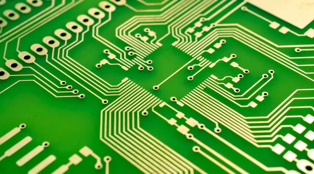
Printed Circuit Board (PCB) assembly is a critical stage in the electronics manufacturing process, where individual components are soldered onto the PCB to create functional electronic devices. As technology continues to advance, so do the techniques and methods used in PCB assembly, driving improvements in efficiency, accuracy, and reliability. In this blog, we delve into the realm of advanced techniques in PCB assembly, exploring how these innovations are transforming the manufacturing landscape and enabling electronics manufacturers to stay ahead of the curve.
Surface Mount Technology (SMT)
Surface Mount Technology (SMT) has revolutionized PCB assembly, offering numerous advantages over traditional through-hole assembly methods. With SMT, components are mounted directly onto the surface of the PCB, eliminating the need for holes and allowing for higher component density and miniaturization. SMT enables faster assembly times, reduced material waste, and improved electrical performance, making it the preferred choice for modern PCB assembly processes.
Automated Assembly
Automation plays a crucial role in enhancing efficiency and accuracy in PCB assembly. Automated assembly machines, such as pick-and-place robots and soldering machines, can quickly and precisely place components onto PCBs with unparalleled speed and accuracy. By automating repetitive tasks, manufacturers can streamline the assembly process, reduce labor costs, and minimize the risk of human error. Automated assembly also enables high-volume production, allowing manufacturers to meet tight deadlines and scale their operations to meet growing demand.
Advanced Inspection Techniques
Quality control is paramount in PCB assembly, and advanced inspection techniques are essential for ensuring the integrity of the finished products. Automated optical inspection (AOI) systems use cameras and image processing algorithms to inspect PCBs for defects such as missing components, misaligned components, and soldering defects. X-ray inspection is another valuable technique that allows manufacturers to inspect the internal structure of PCBs, identifying defects that may not be visible to the naked eye. These advanced inspection techniques enable manufacturers to identify and rectify defects early in the assembly process, ensuring high-quality finished products.
In-Circuit Testing (ICT)
In-Circuit Testing (ICT) is a powerful technique used to verify the electrical integrity of PCBs during the assembly process. ICT involves the use of specialized test fixtures and probes to measure the electrical characteristics of individual components and verify proper connectivity between them. By subjecting PCBs to rigorous electrical testing, manufacturers can identify defects such as short circuits, open circuits, and component failures, ensuring that only fully functional PCBs are shipped to customers. ICT helps manufacturers maintain high standards of quality and reliability while minimizing the risk of costly rework and returns.
Design for Manufacturability (DFM)
Design for Manufacturability (DFM) is a proactive approach to PCB design that aims to optimize the manufacturability of PCBs and minimize the risk of assembly errors. By considering manufacturing constraints and requirements early in the design process, designers can create PCB layouts that are easier and more cost-effective to assemble. DFM principles include optimizing component placement, minimizing the number of unique components, and designing for automated assembly. By incorporating DFM principles into the design phase, manufacturers can streamline the assembly process, reduce production costs, and improve overall product quality.
Lean Manufacturing Principles
Lean manufacturing principles, such as just-in-time (JIT) production and Kanban systems, are increasingly being applied to PCB assembly processes to eliminate waste and improve efficiency. JIT production aims to minimize inventory levels by producing only what is needed, when it is needed, thereby reducing storage costs and minimizing the risk of obsolescence. Kanban systems use visual cues to signal when components need to be replenished, ensuring a steady flow of materials and preventing production bottlenecks. By embracing lean manufacturing principles, manufacturers can optimize their assembly processes, reduce lead times, and improve overall productivity.
Conclusion
In conclusion, advanced techniques in PCB assembly are driving significant improvements in efficiency, accuracy, and reliability in the electronics manufacturing industry. From Surface Mount Technology (SMT) and automated assembly to advanced inspection techniques and Design for Manufacturability (DFM) principles, manufacturers have a wealth of tools and methods at their disposal to optimize the assembly process and deliver high-quality products to customers. By embracing these advanced techniques and incorporating them into their operations, electronics manufacturers can stay competitive in a rapidly evolving market and continue to push the boundaries of innovation in PCB assembly.